Projects Home
Back to Photo List
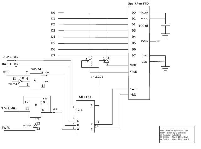
This schematic also began as a Kivio drawing and is not intended to be suitable for gEDA or other schematic/pcb programs. The signal names on the left are those from the H89 header labeled P602. The data lines above that connect to the corresponding data lines on H89 header labeled P601. Power (+5V) for the 74LS125, 74LS138, 74LS74, and 74LS04 is taken from Pin 1 of P602 while ground is from Pin 2.
As with the original prototype, the USB board is a circuit board from SparkFun.com. It has sufficient circuitry to provide choices as to how the board is powered and other options. Not all of the pins of the actual FT245 chip are accessible, but then for our purposes they are not needed. The pins on the board are on .100 inch spacings with a .600 inch separation between the two rows. By connecting the VUSB and VCCIO pins together (and decoupling with a .1 uF (100 nf) capacitor, the board draws it power from the USB connector and not from the Heathkit.
On the Heathkit side (the parallel side), there are no interrupt lines, only two status lines for the FIFO buffer, transmitter empty (TXE) and receiver full (RXF), both of which are "low true." There are pins for Read from the FIFO (RD) and write to the FIFO (WR), also both "low true."
A more complete description of the functioning of the gadget accompanies the code for the H89 device driver at the USB Projects page.